Inspection and review stations for defects review, automated wafer handling for 6" and 8" wafers, free or map driven inspection, bin code re-classification
Read moreMicroscope loaders with macro inspection. Graphical touch screen interface.
LASER mapping for very thin wafers. Up to 200 mm silicon, glass, sapphire wafers. TAIKO, through holes and bonded wafers
UV treatment systems for silicon wafers. UV dicing and grinding tape deactivation, UV - ozone cleaning, Memory erasure. Manual or automatic loading
Read moreThermocouple instrumented wafers for temperature probing in semiconductor production processes.
Different types and sizes of substrates. Maximum temperature from 250 to 1000 °C. K or T thermocouples
Carbon fiber end effectors for wafer handling.
Available as spare parts for existing tools or for OEM applications. Extremely durable and reliable. Low cost of ownership. Versions for critical wafers available. Rapid prototyping service.
Wide range of accessories for semiconductor manufacturing. Bright light inspection illuminators. Wafer handling wands. Vibration insulation tables for microscopes.
Read more
Semisyn is a division of Astel, an R&D company based in Ivrea, Italy.
Working on semiconductor manufacturing market since 1994, we have served the most important semiconductor and electronic components manufacturers for more than twenty years, all over the world.
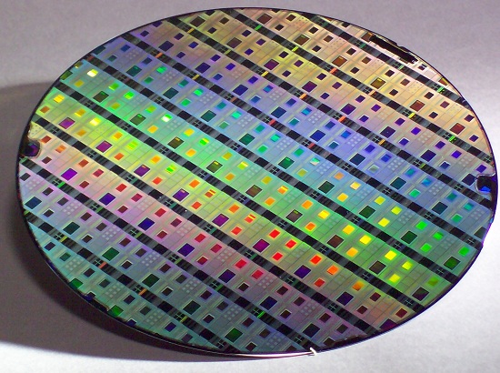
Our products and services cover wafer handling, processing, spare parts and inspection systems, not only semiconductor manufacturing.
Copyright ©2021 - Astel Srl - P.IVA 07083610019
Website by Web&Com


")